Homework 7
Homework 7: Making it count! (or SUMmarizing and re-STATEing )
Goals
The goals of this assignment are to summarize and combine multiple aspects of the course:
- Take another look at a common approach to state machines
- Continue to explore the design of computers by taking a deep look at the control and datapath for a RISC-V single-cycle microarchitecture.
- Look at one way computers can interface with the real world (screens, keys, etc.)
- Ensure everyone has an opportunity to take a digital design and generate real-world hardware that implements that design.
(All of the above are overall learning outcomes for the course)
The goals are:
- Create a short example program, which will need certain instructions to run.
- Update a RISC-V model to support a needed instruction,
lui. - Actually implement it with our hardware!
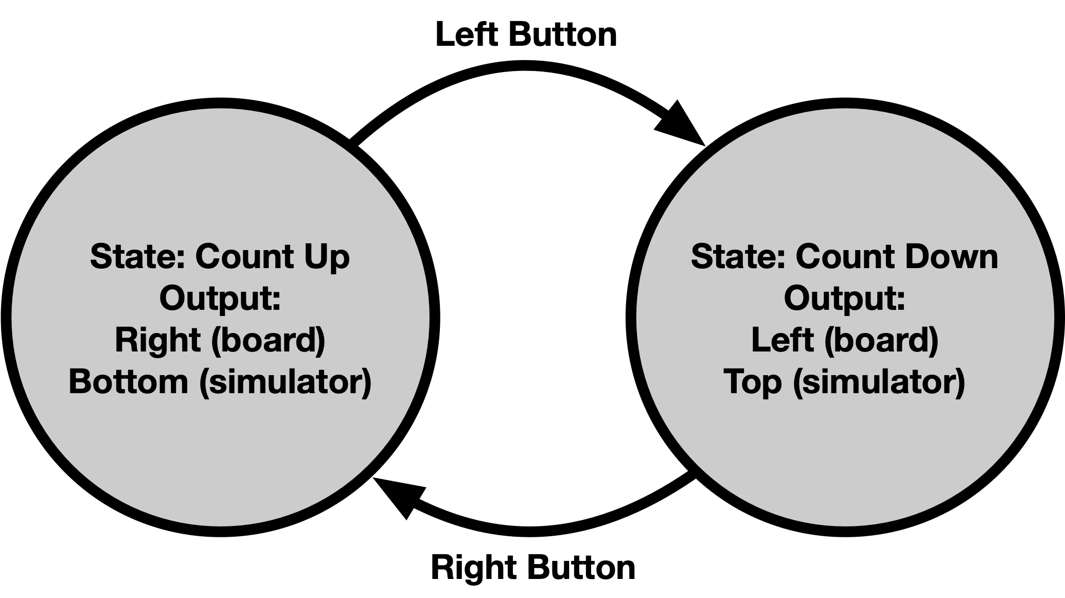
The goal is a very simple state machine that controls a counter. The counter will either count up or count down. The count will be shown on a display, two LEDs will also be used to show which mode it’s in (counting up or counting down), and buttons will be used to switch it between counting modes. (Often when the word “mode” is used in electronics and computing/software, it’s referring to the state of a state machine).
When done it should behave like this:
Part 0: Setup
Link to get the repository / codespace: link
Part 1: Coding a State Machine
Background: Input/Output
We have covered how CPUs interact with memories, but we haven’t covered how they get input from the outside world or how they provide output, the combination commonly referred to as “I/O”. Without I/O computers wouldn’t have much impact.
A form of I/O that’s a variation on things we’ve already seen is “Memory Mapped I/O”. Memory mapped I/O is connected like the RAM. Interaction of the device is just reading from and writing to the RAM locations that correspond to the device. In this case we will designate memory locations for the elements of the Key and LED module:
| Memory Address | What | Read / Write / Both |
|---|---|---|
0x8000 (32'h8000) |
32-bit value that will be displayed on the digits of the display | Read or write |
0x8004 (32'h8004) |
32-bit value; Lowest eight bits control LEDs. Bit 0 is rightmost LED (D8 on the board; LED 1 in the simulator) |
Read or write; Only lowest 8-bits are writeable |
0x8008 (32'h8008) |
32-bit value; Lowest eight bits represent the most recent state of the buttons. Bit 0 is rightmost button (SW8 on the board; Button 1 in the simulator) |
Read only. Writes will be ignored. |
RISC-V assembly language uses the 0x notation to indicate a hexidecimal value. That format should be used for this problem.
In our final computer we can use sw to store values at address 0x8000, which will cause the value to be shown on the screen. Correspondingly, we can read from 0x8004 using lw to determine if any buttons are currently pressed.
State Machines
State machines can also be represented with program code, where a variable typically contains the state (the variable is stored in RAM and that variable is just being used like the flip-flops we’ve used to store state). It’s often much easier to write a computer program for a state machine than it is to create a digital circuit.
Problem 1: RISC-V Assembly State Machine
Here’s a description of the state machine:

- Start by creating a prototype program in the programming language of your choice. You can use whatever technique you want to simulate the “buttons”. (It may be easiest to do something that prompts for the button every time through a loop. Perhaps
0and1could represent the two buttons and if any other key is typed it would indicate neither is pressed) - As in the prior assignment, make a plan to convert your code to assembly language. You’ll need to update your I/O code to use the memory-mapped locations for our display, LEDs, and keys.
- Add your code to the
counting/counting.sproject in the designated places. TheTODOitems indicate where you should initialize values and where your main code (loop) should be. Although our real key/led board will be memory mapped, the simulated one is not. Instead we are emulating memory mapping by thejal update_memmappedinstruction and some additional code. Be sure the that instruction is called everytime you need to update states and output. Eachjal update_memmappedwill synchronize the values at0x8000,0x8004, and0x8008with the simulated display. In most cases it should only be needed one place that happens just after outputs are updated and before the next state is computed.
Caution!
Only use the instructions listed in the file (li, lw, sw, add, sub, and, or, slt, addi, andi, ori, slti, beq, and jal)!
The simulator will open a small, simulated board that operates like the Key & LED board provided in your kit. There are just two buttons, two LEDs, and two digits on the display, but they should behave the same as our board. The display will only be showing the last two digits of the value, but the simulation runs slow enough for that to work well.
Your code should behave like:
Part 2: Adding an Instruction
Caution!
This is a real-world example of a significant computer engineering task. You need to have a plan rather than just opening the Verilog file and typing.
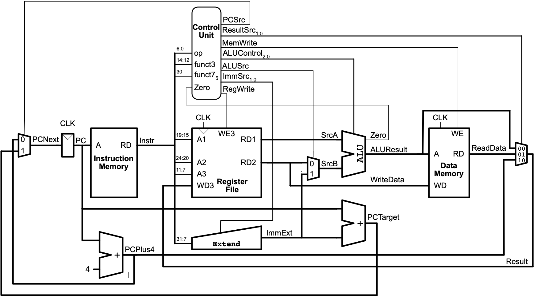
The risc-v folder contains a Verilog implementation of a partial RISC-V processor (an implementation that corresponds to our textbook). It is a single-cycle CPU and includes a full datapath and the elements that control the datapath. It supports only the following instructions: lw, sw, add, sub, and, or, slt, addi, andi, ori, slti, beq, and jal
You probably needed to use an li in your code for part 1. Note that li is a pseudo-instruction that is translated into either addi or a combination of both a lui and an addi (Table B.7). In order to work with our display, we need to access memory address 0x8000-0x8008, which requires the version of li that translates to a lui….And the provided processor does not support lui. You will need to update the processor (control and datapath) to support lui.
- Start with:
- a diagram of the single-cycle CPU:

(Figure 7.15 from Digital Design and Computer Architecture, RISC-V Edition by Harris & Harris)
-
Review
lui, its meaning/behavior (also referred to as its “semantics”), and its format in Figure B.1 and Table B.1 -
You’ll also need to understand how various parts of this CPU implementation that aren’t fully described in the diagram behave. The parts that aren’t shown in the diagram are the ALU (Table 7.3, page 409) and the Extend unit (Table 7.5, page 412).
-
Develop a plan for how the existing design can be modified to support
luiand annotate it on the diagram. It may help to re-read/review 7.3 of the text.Caution!
If you come to office hours or need help on this part, the first question will be “show us your diagram”. We will need to know what you want to do before we can help.
-
Code review: The code in
risc-v/riscvsingle.svreprents a working model of a significant part of a RISC-V CPU. It contains a hierarchy of multiple modules. At the top of that hierarchy is theriscvsinglemodule. It contains the two major aspects of a simple CPU: acontroller, which decodes instructions and configures the other element, thedatapath. As the name implies, thedatapathencompasses all the components that process data.- Review the various modules in
riscvsingle.svand update your diagram with details about which modules correspond to which parts of the diagram. For example, there are actually two Verilog modules that correspond to the “Control Unit”. Also, look carefully for the types of signals that are important for your approach to supportinglui.
- Review the various modules in
- Identify a plan to update
riscvsingle.svto supportlui(there are multiple valid approaches). Updateriscvsingleand check your work with the provided testbenches, which are described in the “Testing” section below.
You may find that you want to “Revert” your changes if things aren’t working out. You can easily retrieve the original code via git or GitHub. Here are two approaches:
- Go to the repository on GitHub.com, click on the file of interest, then click on the
Historybutton, and finally select a specific version to view (if you haven’t pushed updates to GitHub, only the original version will be shown). You can copy/paste the code as needed. - Right-click on a file in the CodeSpace file explorer and select
Open Timeline. ATIMELINEview will be shown in the explorer panes and you can select an older version of the work, which will be compared with the current version. The timeline includes bothgitcommits and the times the file has been saved since you opened the Codespace session.
Testing
Three testbenches are configured:
- risc_v_lui_tb: This just tests a few variations of
luiinstructions. This will help test that yourluiworks without consideration for other instructions. If successful, thePROBLEMSpanel will show an entry forrisc-v-lui-tb.svthat says “All tests passed!”. If not successful, it will contain some details about the specific instruction that failed.- The machine code and assembly language being checked is in
risc-v-lui-tb/lui-test.rom.txt
- The machine code and assembly language being checked is in
- risc_v_getn_tb: This is a more general test. It tries nearly all instructions once, including the
lui. It isn’t a very rigorous test, but it will help confirm that changes toluiprobably didn’t interfer with the behavior of other instructions. If successful, thePROBLEMSpanel will show an entry forrisc-v-gen-tb.svthat says “Simulation succeeded!”.- A copy of the assembly language listing for the program being run is in
risc-v-gen-tb/risc-v-gen.s. If the testbench fails, you may need to refer to the actual instructions to identify bugs. (See “Debugging the Datapath” below). (Changingrisc-v-gen.swon’t have any impact. It was used to create the machine code inrisc-v-gen.rom.txtthat is actually being use by the testbench)
- A copy of the assembly language listing for the program being run is in
- risc_v_counting_tb: Part 1 needs to be completed first and then the
counting: romtask should be run to convert code to an UPduino ROM. This test bench can be used to try to verify that your code is running correctly. You can modify the test case in therisc-v-counting-tb.svfile indicated in theTODOnotes. The “Debugging” video below shows both hwo this works and how you can use the waveform traces to debug flaws in your design.Caution!
Check to see if the
PROBLEMSpanel indicates any errors withcounting.rom.txt. If it indicates your code uses an unsupported instructions (“Line may not contain an allowed instruction”), review and revise your code as needed.
Debugging the Datapath
The “Surfer” waveform view allows you to see the step-by-step execution of a program and look at all components of device under test (that is, the CPU).
Here’s an example of using waveforms to understand what’s going on:
And another example, focused on the lui testbench and how you may want to use the waveforms to understand and debug Verilog:
Part 3: Making it Real
- If you haven’t already done so, do Parts 2-2.1 of Studio 7B. Confirm that the display is connected correctly and works.
- You’ll need to convert your code from Part 1 to machine code (binary) and it will be programmed in the ROM. A task has been provided that will do this for you:
counting: rom. The task will:- Use a real assembler for RISC-V to translate your code to machine code.
- Adjust the format to be suitable to program a “ROM” representation on the iCE40.
- Open a window showing the machine code and the original assembly language. Review the code that’s generated. Confirm that:
- The two “do not edit” parts, the
jalinstruction and the code at the bottom of the file, were removed. - You are only using instructions supported by this simplified RISC-V model (
li,lw,sw,add,sub,and,or,slt,addi,andi,ori,slti,beq,j, andjal)
- The two “do not edit” parts, the
- Once you are sure that your UPduino is connected correctly, your RISC-V model supports
luicorrectly, and that your code is appropriate, use the therisc-v: imagetask to build the image and the web programmer to program it!
Part 4: Reflections & Questions
Answer the questions in questions.md
Submission
You will need to submit your assignment via Gradescope. There will be three distinct dropboxes:
Parts 1-2, 4
As with prior homeworks, work should be submitted via Gradescope. Like in Homework 5, you will need to commit and push work to GitHub and then go to Gradescope to “pull” the work over. You should:
- Submit Part 1 under the appropriate dropbox (confirm the results of the unit testing) (confirm the results of the unit testing)
- Submit Part 2 under the appropriate dropbox (confirm the results of the unit testing).
- Submit Part 4 to the appropriate dropbox
- Confirm that
questions.mdis included and transferred to Gradescope.
Part 3
A demonstration / discussion of your work is required.
You can do a “demo” (brief overiew/discussion of your work) during TA or instructor office hours starting Tuesday, Dec. 3.
Submission time will be based on Gradescope submissions, not the demo time. There will be additional office hour times for demos between Dec. 3 and Dec. 6, some time during the class session on Thursday, Dec. 5th, and during reading days (~10am-5pm the 9th-11th).
- Submission Link: Gradescope
